Super High-Speed Techniques for Spatially Modulated Field Signals
Introduction
The denseness magnification of integration of VLSI elements together with growth of their work action causes the growth of signals space complexity conditioned by electromagnetic interconnections, Ferry et al. A special discretec haracteristic of spatially modulated field - the topological scheme - was offered to use for the purposes of digital information input. The earlier developed theory (topological approach for boundary problems of an electrodynamics) has allowed to make a conclusion about a possibility of fulfillment for some logic operations with the help of passive (strip) components. The first device simulation outcomes which permits to switch it with subpicosecond speed in different stratums of the three-dimensional signal circuit depending on space topology, are considered in recent author's papers (1992-1998).
Physical analysis and theoretical results
The present article purpose is to research three main problems in this area: influence of solid-state effects in conductors and dielectrics on signals processing processes, creation of perspective subpicosecond element basis for digital processing of the spatially-modulated signals and problems of new elements integration in perspective VLSI.
The essential influence upon perspective elements performances have the physical effects in solid-states and diffractional phenomena on strip transmission line discontinuities in subpicosecond modes area of signals processing. By the outcomes, indicated in Table 1, of the analysis of various physical effects, on the basis of micron strip engineering the creation of unquantum circuit components with subpicosecond speed is possible. The Table was composed by using different papers and books.
Table 1. Time scales of main physical effects in IC elements
|
№ |
Physical effect |
Time or frequency evaluation of an effect |
|
|
Limited mode velocity in microstrip transmission lines. Time delay of signal in a microstrip transmission line on the substrate with dielectric permittivity e: |
~ 33.3 Ц e , fs/m m |
|
|
Inertia of interaction of electromagnetic field with free charge in the region of low values of photon energy. |
Defined by efficient or free mass of charges |
|
|
Maxwell relaxation time of charges in conductors: |
~ 0.001 – 0.01 fs |
|
|
Collective effects in the electronic plasma. |
~ 0,067 – 0,2 fs |
|
|
Relaxation phenomenas in dielectric. Time constant of electronic |
~ 1 – 10 fs ~ 10 – 10000 fs |
|
|
Minimal time of transition an electron from one energy level on the another in atom: |
~ 1 – 10 fs |
|
|
Typical theoretical time of electron relaxation in quantum nanoelements: |
|
|
|
Electron-phonone interaction. |
~10 THz |
|
|
Transient-time effects on discontinuities of strip transmission lines of micron sizes. |
~ 80-150 fs |
|
|
Excitation of higher modes on discontinuities of microstrip transmission lines in VLSI. Cut-off frequency of the first higher mode: |
~ 10- 100 THz |
|
|
Excitation of surface waves in micron microstrip transmission lines. Critical coupling frequency of the strip and surface modes: |
|
The digital components for processing spatially - modulated signals are constructed on the base of the usage of field topology for input, transfer and information processing. A typical signal of a similar kind can be a sequence of impulses even (logic 1) and odd (logic 0) modes in coupled strip transmission lines (Fig. 1,a,b).
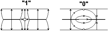
(Fig. 1,a,b)
The number of logic operations above such signals manages to be realized without use of semiconductor elements with significant time delay. On Fig. 2 the switch permitting to switch logic signals (impulses of even and odd modes of micron-sized coupled strip transmission lines) into different layers of the three-dimensional circuit is represented.
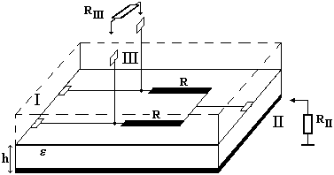
(Fig. 2)
Its truth-table is shown on Fig. 3.
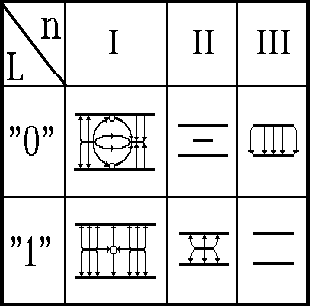
(Fig. 3)
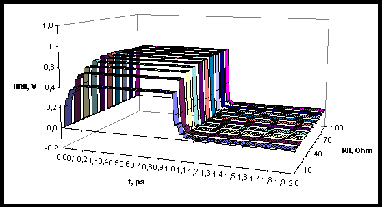
In the equivalent circuit the final sizes of resistors R and their parasitic edge-end reactivities were taken into account according to Easter. The duration of transients for signal switching of a rectangular signal did not exceed several fractions of picisecond, and the time delay of it was no more than 0.03 ps for resistor R length 1 mkm (Fig.4 a, b).
a)
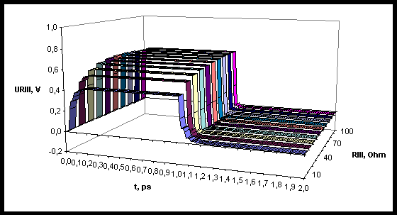
b)
Fig. 4.
Transient characteristics of the switch for topologically modulated signals. a) Output signal on the port II
(logical 1 on the input I). b) Output signal on the port III (logical 0 on the input I). R=18 Ohm e =3.5, h=3 mkm, Ze=84.32 Ohm, Zo=47.85 Ohm.
The settlement energy costs to fulfill that operation have appeared on the order smaller, than for transistor analogs (Fig. 5).
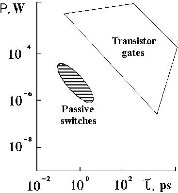
(Fig. 5)
Time-energy performances of switches for topologically modulated field signals and their transistors analogs.
Application of the new super-high speed circuits
The article discusses the new VLSI concept, taking into account the tendency to create three-dimensional circuits with superdense elements accommodation. The evaluations specify, that owing to electromagnetic interinfluences space frequency of signals fields in electronic IC may be compared to a bit density in the optical three-dimensional holograms. It is offered to design the perspective specialized electronic IC on the basis of simulation of the holographic effects in picosecond impulses frequency band with the usage of a similarity method. The principle of a field topological modulation will allow to use digital methods to realize holographic principles of construction for the new circuits. Thus, the number of processing signal operations is offered to be executed at the expense of superfast effects such as a diffraction of waves on strip components, and other necessary operations, for example, management of interconnections structure, switching of compared images frames, amplification and signals generation to realize with the help of semiconducting components. The given IC architecture and the principles of its work will allow to unite functional advantages of the electronic and optical circuits during spatially - modulated signals processing. This report will discuss the circuitry solutions from this area.
Conclusion
Method and circuitry of superfast (subpicosecond logic processing of spatially (topologically) modulated signals by the passive strip components were considered. The evaluations of physical effects influencing on time processes of picosecond signals processing were indicated. The conclusion about a basic possibility of creation of strip circuits with subpicosecond speed was made. The outcomes about theoretical modeling of the topologically modulated signals switch were discussed. The new concept of superdense IC, constructed on the basis of holographic effects physical analog-digital modeling for the topologically modulated signals was developed.